Main Menu


.png)


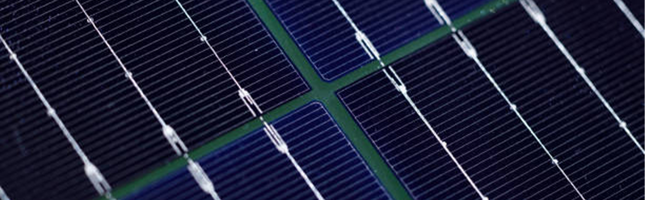
Understanding Passivation Technology: The Path to Enhancing PV Cell Efficiency

I.Why Do PV Cells Need Passivation?
Efficiency is the eternal pursuit of PV cells, as this critical indicator directly determines their competitiveness and application prospects in the energy market. In the ongoing quest to boost efficiency, we must confront the various obstacles PV cells face during operation—their efficiency losses primarily stem from two sources: optical losses and electrical losses.
Optical losses are largely caused by shading from the metal grid lines on the cell surface. When sunlight hits the cell, the areas covered by metal grid lines cannot effectively absorb photons and convert them into electricity, resulting in wasted light energy.
Electrical losses, by contrast, are more complex. One part arises from contact resistance between the metal grid lines and the silicon wafer. When electrons travel across the interface between the metal grid lines and the silicon wafer, differences in material properties create resistance that hinders smooth electron flow, leading to energy loss. The other part of electrical losses comes from recombination losses of electrons and holes. In silicon wafers, after photo-generated carriers (electrons and holes) are produced, if they recombine before reaching the electrodes, they cannot contribute to the photo-generated current—thus reducing cell efficiency. Recombination of electrons and holes may occur in the bulk material of the silicon wafer, but it is more prevalent on the wafer’s surface and at the contact points between the wafer and metal. For example, the silicon wafer surface contains numerous dangling bonds and defects, which act as traps for carriers, causing electrons and holes to recombine here. This significantly shortens carrier lifetime and degrades cell performance.
Passivation technology is therefore crucial for improving PV cell efficiency, primarily addressing electrical losses—especially reducing electron-hole recombination. Simply put, passivation technology involves applying a special material layer on the silicon wafer’s surface or specific regions. This layer “covers up” the defects on the silicon surface that easily cause electron-hole recombination. For instance, materials like aluminum oxide (Al₂O₃) and silicon nitride (SiNₓ) form a film on the silicon wafer surface. Aluminum oxide films, for example, are highly stable and can bond with surface defects on the silicon wafer, making it harder for electrons and holes to recombine. This extends the lifetime of photo-generated carriers (electrons and holes) in the silicon wafer—a parameter known as minority carrier lifetime.
Experiments show that after aluminum oxide passivation, minority carrier lifetime can increase from several tens of microseconds to several hundreds of microseconds. A longer minority carrier lifetime directly raises the open-circuit voltage (VOC)—a key indicator of cell performance closely linked to output power. Typically, every 10mV increase in open-circuit voltage boosts the cell’s photoelectric conversion efficiency by 0.4%–0.6%.
Another example is Tunnel Oxide Passivated Contact (TOPCon) technology, which inserts an ultra-thin silicon oxide layer and a heavily doped polysilicon film between the silicon wafer and metal. This acts like a “fast, smooth path” for electrons: electrons can travel quickly through it while recombination losses are reduced. This improves the cell’s ill factor (FF)—a metric reflecting the ratio of the cell’s actual output power to its theoretical maximum output power. A higher fill factor means the cell’s actual output power is closer to its theoretical maximum, thereby enhancing overall efficiency. PV cells using TOPCon technology can achieve a fill factor of 82%–84%, with efficiency improved by 1–2 percentage points.
II.The Principle of Passivation Technology
To understand how passivation technology works, we first need to grasp the carrier recombination mechanism. Silicon wafers are the core material of PV cells. When illuminated, electrons in the valence band of the silicon wafer absorb photon energy and jump to the conduction band, generating electron-hole pairs. These electrons and holes must be separated and collected to form an electric current—but in reality, they tend to recombine easily.
There are three main types of carrier recombination:
- Radiative recombination: When electrons and holes recombine, they emit a photon. In solar cells, this represents energy loss.
- Auger recombination: During recombination, excess energy is transferred to another carrier, exciting it to a higher energy level. This type of recombination is more likely to occur in regions with high carrier concentrations.
- Recombination via defect states: The most common and impactful type. Silicon wafers (both surface and interior) contain various defects—such as incomplete crystal structures and impurity atoms. These defects form energy levels within the silicon’s bandgap, acting as “recombination centers.” Electrons and holes can recombine through these centers, drastically shortening carrier lifetime.
The silicon wafer surface has a high density of dangling bonds due to the abrupt termination of its crystal structure. These bonds act like “traps” that easily capture carriers, leading to a much faster surface recombination rate than in the wafer’s interior. Additionally, when the silicon wafer comes into contact with metal electrodes, metal impurity atoms can diffuse to the wafer surface, increasing surface defects and exacerbating recombination.
Passivation technology aims to reduce the carrier recombination rate and improve cell performance. It mainly falls into two categories: chemical passivation and field-effect passivation.
- Chemical Passivation
Chemical passivation uses chemical substances to react with defects and dangling bonds on the silicon wafer surface, reducing the density of surface states and minimizing recombination centers. For example, silicon nitride (SiNₓ) films are commonly deposited on silicon wafers using Plasma-Enhanced Chemical Vapor Deposition (PECVD). During this process, hydrogen atoms in the SiNₓ film bond with dangling bonds on the silicon surface to form Si-H bonds, “filling” the dangling bonds and significantly reducing surface state density. Meanwhile, the negatively charged SiNₓ film creates an electric field on the silicon surface, repelling minority carriers (holes in n-type silicon wafers, electrons in p-type silicon wafers) and reducing their probability of recombining on the surface.
- Field-Effect Passivation
Field-effect passivation creates an electric field on the silicon wafer surface to alter carrier distribution and reduce recombination. The tunnel oxide passivated contact structure in TOPCon technology is a typical example. On the back of a TOPCon cell, an ultra-thin silicon oxide (SiO₂) layer (approximately 1–2 nm thick) is first deposited. This layer exhibits the quantum tunneling effect: electrons can pass through it, but holes cannot. A layer of heavily doped polysilicon (Poly-Si) is then deposited on top of the silicon oxide. The polysilicon contains a large number of free electrons, forming an accumulation layer at the SiO₂-Poly-Si interface. The electrons in this accumulation layer create an electric field on the SiO₂ surface, repelling holes and reducing electron-hole recombination in this region. At the same time, the heavily doped polysilicon layer provides an excellent conductive path for electrons, allowing them to quickly transfer to the metal electrodes. This avoids the high recombination losses caused by direct contact between silicon and metal. Through the combined action of the silicon oxide layer and the heavily doped polysilicon layer, TOPCon cells achieve excellent passivation and contact performance, boosting efficiency.
III. Common Passivation Technologies for PV Cells
- Aluminum Oxide (Al₂O₃) Back Passivation
Aluminum oxide (Al₂O₃) back passivation is widely used in high-efficiency PV cells, such as Passivated Emitter and Rear Cell (PERC) technology. During cell manufacturing, Atomic Layer Deposition (ALD) is typically used to deposit the Al₂O₃ passivation film. The ALD process works like “building blocks”: reactive gases are deposited on the silicon surface one atom at a time. First, an aluminum source gas (e.g., trimethylaluminum) is introduced, forming a monolayer of aluminum atoms on the silicon surface. Then, an oxygen source gas (e.g., ozone) reacts with the aluminum to form aluminum oxide. This cycle is repeated hundreds of times to grow an Al₂O₃ film 5–10 nm thick.
Aluminum oxide is insulating and stable, preventing charge recombination on the back of the silicon wafer. It saturates dangling bonds on the silicon surface, reducing surface defect density. Additionally, the fixed negative charges in the Al₂O₃ film create a strong electric field on the silicon surface, repelling minority carriers (holes in n-type silicon wafers) and lowering the surface recombination rate.
Experiments show that PERC cells with Al₂O₃ back passivation can reduce the backside recombination rate to 10–100 cm/s. This increases the open-circuit voltage by 20–30 mV, improves short-circuit current density, and enhances the fill factor—ultimately boosting photoelectric conversion efficiency by 1–2 percentage points. Today, Al₂O₃ back passivation technology is mature; with improvements in ALD equipment and process optimization, costs have decreased, making it increasingly widely used in large-scale production.
- Silicon Nitride (SiNₓ) Passivation
Silicon nitride (SiNₓ) passivation is a long-standing and widely adopted technology that improves both the optical and electrical performance of PV cells. SiNₓ passivation films are usually deposited using PECVD. Inside a PECVD chamber, reactive gases (e.g., silane, ammonia) are ionized into plasma under radiofrequency (RF) electric fields. These reactive particles react and deposit a SiNₓ film on the silicon wafer surface. By adjusting parameters such as gas flow rate, RF power, and deposition temperature, the composition, thickness, and optical/electrical properties of the SiNₓ film can be controlled—with typical film thickness ranging from 60–80 nm.
SiNₓ films have excellent light transmittance, with an average transmittance of over 90% in the visible light range—ensuring they do not hinder light absorption by the cell. Electrically, hydrogen atoms in the SiNₓ film are critical for passivating the silicon surface. During deposition, a large number of hydrogen atoms are incorporated into the film and bond with dangling bonds on the silicon surface to form Si-H bonds, reducing surface state density. Moreover, the negatively charged SiNₓ film creates an electric field on the silicon surface, minimizing minority carrier recombination.
In the past, SiNₓ passivation was commonly used in crystalline silicon solar cells to enhance efficiency. Today, it is still used for front-side passivation in many high-efficiency monocrystalline silicon cells, where it serves both as an antireflection coating and a passivation layer. Experimental data shows that after SiNₓ passivation, the surface state density of silicon wafers can be reduced to 10¹²–10¹³ cm⁻², and the surface recombination rate to 10²–10³ cm/s. This increases the open-circuit voltage and improves short-circuit current density (due to better light absorption and carrier collection), enhancing overall cell performance. With its simple process and low cost, SiNₓ passivation is well-suited for large-scale production and remains a key technology in the PV industry.
- Tunnel Oxide Passivated Contact (TOPCon) Technology
TOPCon technology is a high-efficiency PV cell technology that has developed rapidly in recent years, with its unique passivated contact structure being its core advantage. TOPCon cells typically use n-type silicon wafers. On the back of the cell:
- An ultra-thin silicon oxide (SiO₂) layer (1–2 nm thick) is first grown via thermal oxidation or plasma oxidation. This layer exhibits the quantum tunneling effect—allowing electrons to pass through while blocking holes.
- A 100–200 nm thick layer of heavily doped polysilicon (Poly-Si) is then deposited on the SiO₂ using Chemical Vapor Deposition (CVD). The heavily doped polysilicon contains a large number of free electrons, forming an accumulation layer at the SiO₂-Poly-Si interface.
The passivated contact structure of TOPCon reduces recombination through three key mechanisms:
- Tunneling effect: The ultra-thin SiO₂ layer enables electrons to pass through via quantum tunneling, while blocking holes—minimizing electron-hole recombination losses. By optimizing the thickness and quality of the SiO₂ layer, the electron tunneling probability can be maximized while blocking holes, reducing recombination current.
- Field passivation effect: Electrons in the heavily doped polysilicon layer create a strong electric field on the SiO₂ surface, repelling holes. This makes it difficult for holes to approach the SiO₂-silicon interface, drastically reducing electron-hole recombination in this region. With the TOPCon structure, the backside recombination rate of cells can be reduced to 10–100 cm/s—far better than traditional direct metal-silicon contact structures.
- Excellent electron conductivity: The heavily doped polysilicon layer provides an efficient conductive path for electrons. Metal grid lines on the back of the cell contact the polysilicon layer (instead of directly contacting the silicon wafer), avoiding surface recombination losses caused by metal impurities. The high conductivity of the polysilicon layer allows electrons to quickly transfer to the metal electrodes, improving the cell’s fill factor and output power.
Currently, the industry primarily uses two methods to deposit the ultra-thin SiO₂ tunnel layer and doped polysilicon layer: Low-Pressure Chemical Vapor Deposition (LPCVD) and PECVD:
LPCVD: Enables precise control of film growth and produces high-quality films. However, it has drawbacks such as short quartz tube lifespans (requiring frequent replacement), high costs, and susceptibility to dust in the furnace tube (which affects the quality of the backside tunnel layer).
PECVD: Allows low-temperature deposition and high production efficiency. However, it may suffer from issues like “pinpoint defects” and uneven passivation effects—requiring process and equipment optimization to resolve.
With technological advancements, TOPCon efficiency continues to improve: laboratory efficiency has exceeded 26%, and mass-production efficiency reaches approximately 24%–25%. It has become one of the mainstream technologies in the PV industry.
- Heterojunction (HJT) Technology
Heterojunction (HJT) technology—officially known as crystalline silicon heterojunction solar cell technology—features a unique structure and distinct advantages. Its cell structure consists of amorphous silicon films and transparent conductive oxide (TCO) films deposited on both sides of a crystalline silicon wafer:
– The amorphous silicon films form a heterojunction with the crystalline silicon, effectively reducing surface recombination. Additionally, the intrinsic layer of the amorphous silicon films acts as a passivation layer, minimizing carrier recombination.
– The TCO films are both transparent and conductive: they allow light to pass through while conducting the generated current out of the cell.
HJT technology offers high cell efficiency (mass-production efficiency of 24%–25%, with even higher laboratory efficiency), low process temperatures (reducing damage to silicon wafers), and compatibility with other technologies for further efficiency gains. Although its cost is relatively high, costs are gradually decreasing with technological development—making HJT highly promising in the PV market.